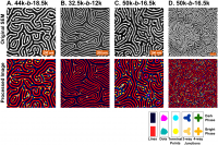
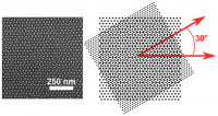
Fabrication of nanoscale features integrated with a range of technologically important semiconductor surfaces, on a sub-100 nm length scale, is a rapidly growing area of research with respect to future semiconductor applications, including hybrid semiconductor-organic and nanoparticle devices, tissue integration, molecular electronics, micro- and nanofluidics, sensing, photovoltaics, and others. Lithography is the single most expensive cost factor in chip manufacturing. To be considered viable from a commercial perspective in the near to mid-term, and beyond, new lithographic approaches should ideally be compatible with existing silicon-based micro- and nanofabrication techniques, presently in operation. Because of the ubiquity of polymers in silicon fabrication (as photoresists, for example), polymer self-assembly to produce nanoscale structures has recently emerged as a possible approach to the production of uniformly patterning broad areas of surfaces. Block copolymer self-assembly is explicitly mentioned in the Semiconductor Industry Association Roadmap as a potential “innovative technology” may be utilized to produce sub-45 nm features on integrated circuits (ICs). In this project, we are developing a number of ways to “convince” block copolymers to form beautiful, complex and useful patterns, with the goal of integrating these processes into chip manufacturing lines on silicon.


